Is this the same phone as the one in your previous question (What should I do to fix that pad?)?
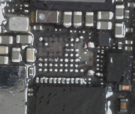
This board has a lot of damage, you have multiple pads that ripped off the board, including the pads for the two capacitors. This is a sign that you are pulling the IC before the solder has molten completely. I'll restate what I said in the previous Q:
Pulling an IC before all of the solder is molten will pull pads. You have to insure the IC floats on the molten solder. You can do this by gently tapping the IC to see if it springs back. Also, avoid wicking. These pads are simply too small and have very little adhesive and copper holding them in place.
What kind of equipment are you using and what temperature and airflow settings are you using? Everyone develops their own style, microsoldering is as much an art as it is a science, but there are some ground rules you have to follow:
- Apply flux and heat ~360-380C to remove the IC. Don't pull or push it with any force until you can see it floating on the melted solder (a slight nudge to see if it moves)
- As much as possible, lift the IC as opposed to pulling it sideways
- Clean the pads of any lead-free solder. Don't wick directly as it damages these delicate pads. You can wick with a fan like method or simply use a concave iron tip to absorb the old solder and use the same tip to apply fresh leaded solder.
- Clean with IPA and inspect under magnification to see if any traces, pads or components were damaged or removed
- Apply fresh flux and set the new IC...apply 360-380C heat. When the solder has melted, the IC should float and properly position itself.
- Clean and test
Obviously, too much heat can cause damage not only to the IC you are replacing but also the surrounding area and the flip side of the logic board. Sometimes passives get disconnected electrically even though they look okay. Those that are encapsulated in underfill are more prone to that.
Also, when testing for "float", we can sometimes nudge the IC too far and cause a solder bridge underneath the IC, shorting out pins that can cause all kinds of problems.
Finally, practice on dead boards until it works well. Don't "learn" on customer devices.
War diese Antwort hilfreich?
Bewertet
Rückgängig machen
Bewertung
3
Abbrechen
Schau durch den Thread, bis du den richtigen Platz für diesen Kommentar gefunden hast. Klicke dann auf "Den Kommentar diesem Post zuordnen", um ihn zu verschieben.