Zum Hauptinhalt wechseln

Der Razer Kishi, ein universeller Mobile Gaming-Controller, der für die meisten Smartphone-Geräte passt, wurde so konzipiert, dass er dir beim Mobile Gaming die gleiche Kontrolle wie bei einer Konsole bietet. Er kam im Juni 2020 auf den Markt.

11 Fragen Alle anzeigen

What pins does the USB-C breakout board hook up to?

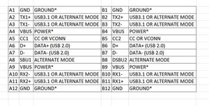
So, my controller's USB-C connection port decided to break off, and I am trying to replace it myself, but my issue is I can not verify 100% what each pin on the breakout goes to on a USB-C male port. So far I have:

TP1 - B4/B9 (VBUS)

TP18 - ?

TP11 - B7

TP5 - B6

TP3 - B5

TP13 - B4/B9 (VBUS)

TP16 - B12 (GROUND)

TP(X) is the labeling on the breakout board itself. Any help would be appreciated

EDIT: image links added here:
https://guide-images.cdn.ifixit.com/igi/...

https://guide-images.cdn.ifixit.com/igi/...

Block Image

Block Image

Diese Frage beantworten Ich habe das gleiche Problem

Ist dies eine gute Frage?

Bewertung 1
2 Kommentare

souswodaem1 post a couple of good pictures with your QUESTION. It might make it easier to properly identify what it is that you are describing. Bilder zu einer vorhandenen Frage hinzufügen

von

Oh that would probably be helpful. I found some images from the IFixIt guide itself:

https://guide-images.cdn.ifixit.com/igi/...

https://guide-images.cdn.ifixit.com/igi/...

they refer to it as the "phone connector" on the service guide. My issue is basically the USB C header came off, and for me to make a new one, I need to know where the pins on the USB C port correspond to the 7 pins on the breakout.

von

Einen Kommentar hinzufügen

2 Antworten

Hilfreichste Antwort

souswodaem1 use your ohm meter and go from the USB C connector to the TP connector and see where each one terminates. Then use the standard USB C wiring to determine which connection that is and where it connects to the TP.

Block Image

War diese Antwort hilfreich?

Bewertung 1

5 Kommentare:

So, I did some experimenting, and I seemingly was getting the same connections as I already deduced, as far as I am aware. Since the board is kinda trashed anyways, I thought I would do an experiment and I sanded off the outer coating, revealing the traces themselves.

https://imgur.com/gallery/HBdAiAm

Seems that the little white lines on the underside of the 7 pin connector indicate which pad that segment is connected too.

So from top to bottom (based off the orientation in my photos), you have the first pin, TP16, being connected to the ground on a USB-C port, then the next pin, TP13, connects to the 4th USB-C pin, which is VBUS.

My only issue is, I can not really see what is supposed to connect on the top side of the connector, as you can see from my photos, I kinda FUBARed the pads when trying to repair it originally. Theoretically since I know how everything paths out on one side, it ideally would match the other side correct?

von

Well, this might have been the most unique way I have ever had to troubleshoot something, but photoshop came to the rescue! With a little bit of the worst photoshop ever, I have come up with this:

https://imgur.com/gallery/YHU5qrK

I took the pins from the good side, added some opacity, and made them line up with what we see on the other side. Doing this, plus a little more testing with the ohm reader, we can see that TP18 DOES in fact have a connection, and it seemingly is connected to the A5 USB-C pin.

von

Is there a reason I would have a pin for A5 and a pin for B5? wouldn’t A5 and B5 be interchangeable? I ask because my USB-C Male PCB board only gives me access to one set of pads, so, if I were to wire up TP18 and TP3 to this PCB, they would be fighting over one pad.

I guess if they need to be separated I can try to get a jumper from the leftover pin (let's say it is TP3) and jump it to the other CC/VCONN. My assumption is, A5 and B5 work together, and if A5 is CC, then B5 is VCONN. Then if you flip the C connector, that same pin I called A5 is now VCONN, and the same pin I called B5 is now CC.

I think that is why I kept getting confused, because I was assuming the USB-C male pads had different names, when in reality, the pad in the top left is A12, and the pad in the bottom left is B1, no matter which side of the connector is facing up. Huh, that is super cool.

von

souswodaem1 great way using photoshop to discover the traces as well as removing the mask from the board. If I follow your assumptions, seems to make perfect sense as well. I am convinced that you are on the right track and that you are going to get this done. Excellent troubleshooting. Don't forget to keep track of all your step and document those. Think about creating a guide on how you did all of this.It will surely help somebody else out. https://www.ifixit.com/Guide/new

von

Definitely will do! Going to have to practice my soldering for those tiny pads, but I think I can get this done. Thank you again for all of your help, I'll be sure to post some progress when I get everything together

von

Einen Kommentar hinzufügen

I did a continuity yesterday with a cut wire plugged into it to see which of the 4 wire connected to which of the 7 pins and the results were

Tp1 - red

Tp18- unused

Tp11 - white

Tp5 -green

Tp3 - unused

Tp13 - red

Tp16 - black

Not sure of the two unused pins are something my standard usba 3.0 cable didn't support but the controller functioned through the connection before I cut the wire.

War diese Antwort hilfreich?

Bewertung 1
Einen Kommentar hinzufügen

Antwort hinzufügen

souswodaem1 wird auf ewig dankbar sein.
Seitenaufrufe:

Letzte 24 Stunden: 3

Letzte 7 Tage: 5

Letzte 30 Tage: 15

Insgesamt: 477